+7 (812) 645-08-06
FEM microscopes, X-ray microscopes, Electron microscopes
select brand

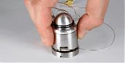
AFM microscope / atomic force - attoAFM I
The attoAFM I is a compact atomic force microscope designed particularly for applications at low and ultra low temperatures. The instrument works by scanning the sample...
AFM microscope / atomic force - attoAFM I
The attoAFM I is a compact atomic force microscope designed particularly for applications at low and ultra low temperatures. The instrument works by scanning the sample below a fixed cantilever and by measuring its deflection with highest precision using a fiber based optical interferometer. Both contact and non-contact mode are applicable. Furthermore, this system is suited for Magnetic Force Microscopy (MFM), Electric Force Microscopy (EFM), and other imaging modes.
The extreme stability of the measurement head allows also for combination with cryogen free pulse-tube based cooling systems for applications where liquid Helium is not available or desired.
The extreme stability of the measurement head allows also for combination with cryogen free pulse-tube based cooling systems for applications where liquid Helium is not available or desired.
Scanning electron microscope / SEM / atomic force / AFM - attoAFM/SEM
With a decade of experience in scanning probe microscopy, attocube has succeeded in equipping the attoAFM I with all the virtues important for successful operation inside a scanning electron microscope (SEM). Thanks to its extremely rugged design and miniaturized size, the force microscope can be fully integrated into almost any SEM currently available on the market. Once mounted inside the electron...
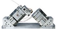
Scanning tunneling microscope / STM - attoSPHERE
The attoSPHERE is a scanning tunneling microscope, designed particularly for room temperature application in demanding conditions, including variable temperature environments and facilities with non-ideal mechanical damping. With its unique material combination, almost exclusively consisting of Invar and ceramics,...
Scanning tunneling microscope / STM - attoSPHERE
The attoSPHERE is a scanning tunneling microscope, designed particularly for room temperature application in demanding conditions, including variable temperature environments and facilities with non-ideal mechanical damping. With its unique material combination, almost exclusively consisting of Invar and ceramics, and its thermally compensated cylindrical design, the attoSPHERE allows the user to obtain atomic resolution images in no time - even in non-ideal lab conditions. With its plug-andmeasure capabilities, the attoSPHERE is ideally suited for topographic and spectroscopic measurements, rapid process control, failure analysis in nanoelectronics, and fundamental research applications. The attoSPHERE is compatible with the highest class cleanrooms and high vacuum conditions.
Principle - The attoSPHERE consists of a cylindrical microscope head which rests self-centered on a sample platform. The microscope head can simply be lifted off for rapid sample exchange. A specifi cally developed coarse positioner allows to approach the STM tip with highly repetitive steps of 75 nm size towards the sample. A fast feedback loop and high repition rates allow to conduct this coarse approach in a matter of minutes.
Principle - The attoSPHERE consists of a cylindrical microscope head which rests self-centered on a sample platform. The microscope head can simply be lifted off for rapid sample exchange. A specifi cally developed coarse positioner allows to approach the STM tip with highly repetitive steps of 75 nm size towards the sample. A fast feedback loop and high repition rates allow to conduct this coarse approach in a matter of minutes.

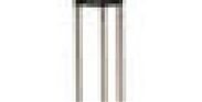
AFM microscope / atomic force - attoAFM III
The attoAFM III is an atomic force microscope designed particularly for applications at low and ultra low temperature. Due to the non-optical shear force detection based on a tuning fork, this system is...
AFM microscope / atomic force - attoAFM III
The attoAFM III is an atomic force microscope designed particularly for applications at low and ultra low temperature. Due to the non-optical shear force detection based on a tuning fork, this system is ideally suited for applications where input of light is problematic. A typical application of the attoAFM III microscope is Scanning Gate Microscopy (SGM) on semiconductor structures. This microscope is also compatible with the commercially available Akiyama probe.
01 LT and HV compatible feedthroughs
02 vacuum window
03 microscope insert
04 superconducting magnet (optional)
05 liquid He dewar (optional)
06 ultra stable Titanium housing
07 xyz coarse positioners
08 xy scanner
09 sample
10 tuning fork including LT compatible preamplifier
01 LT and HV compatible feedthroughs
02 vacuum window
03 microscope insert
04 superconducting magnet (optional)
05 liquid He dewar (optional)
06 ultra stable Titanium housing
07 xyz coarse positioners
08 xy scanner
09 sample
10 tuning fork including LT compatible preamplifier
Atomic force microscope / AFM - attoAFM/STM
In the attoAFM/STM, the two worlds of atomic force and scanning tunneling microscopy are genuinely combined. In contrast...
Atomic force microscope / AFM - attoAFM/STM
In the attoAFM/STM, the two worlds of atomic force and scanning tunneling microscopy are genuinely combined. In contrast to the attoAFM III, the attoAFM/STM uses a horizontally aligned tuning fork to reduce unshielded tunneling current wire length to a minimum (several millimeters in this case).
With this instrument, scanning tunneling spectroscopy measurements on generally non-conductive samples with conductive patches finally become possible.
With this instrument, scanning tunneling spectroscopy measurements on generally non-conductive samples with conductive patches finally become possible.


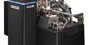
Scanning probe microscope / SPM - LEAP 4000X HR
High Performance 3D Atom Probe for Advanced Materials and Metals Applications
The LEAP 4000X HRTM is a high performance 3D atom probe microscope which provides nano-scale surface, bulk and interfacial materials analysis of simple and complex structures with atom by atom identification and accurate spatial...
The LEAP 4000X HRTM is a high performance 3D atom probe microscope which provides nano-scale surface, bulk and interfacial materials analysis of simple and complex structures with atom by atom identification and accurate spatial...
Scanning probe microscope / SPM - LEAP 4000X HR
High Performance 3D Atom Probe for Advanced Materials and Metals Applications
The LEAP 4000X HRTM is a high performance 3D atom probe microscope which provides nano-scale surface, bulk and interfacial materials analysis of simple and complex structures with atom by atom identification and accurate spatial positioning.
The system works using the principle of field evaporation, whereby a strong electric field applied to the specimen is sufficient to cause removal of atoms by ionization. Atom removal is triggered either via a voltage or laser pulse applied to the sample.
The LEAP HR provides the following key features:
Excellent field of view with good mass resolution
Local electrode and microtip compatibility
Local Electrode and Microtips
"LEAP" is derived from Local ElectrodeTM Atom Probe. The Local ElectrodeTM provides a strong technological advantage over systems which do not have one, improving both ease of use and data quality. The Local Electrode also enables the use of prefabricated MicrotipTM arrays. Using these enables multiple analytical specimens to be prepared, mounted and loaded into the instrument for maximum efficiency with multi experiment scenarios.
Scanning probe microscope / SPM / high-resolution - LEAP 4000X Si
High Performance 3D Atom Probe for Semiconductors, Electronic Devices, and Nanomagnetics
The LEAP 4000X SiTM is a high performance atom probe microscope which provides nano-scale surface, bulk and interfacial materials analysis of simple and complex structures with atom-by-atom identification and accurate spatial positioning.
The system works using the principle of field...
The LEAP 4000X SiTM is a high performance atom probe microscope which provides nano-scale surface, bulk and interfacial materials analysis of simple and complex structures with atom-by-atom identification and accurate spatial positioning.
The system works using the principle of field...
Scanning probe microscope / SPM / high-resolution - LEAP 4000X Si
High Performance 3D Atom Probe for Semiconductors, Electronic Devices, and Nanomagnetics
The LEAP 4000X SiTM is a high performance atom probe microscope which provides nano-scale surface, bulk and interfacial materials analysis of simple and complex structures with atom-by-atom identification and accurate spatial positioning.
The system works using the principle of field evaporation, whereby a strong electric field applied to the specimen is sufficient to cause removal of atoms by ionization. Atom removal is triggered either via a voltage or laser pulse applied to the sample.
Leap Si analysis - dopant in ultra shallow junction specimentThe LEAP Si provides the following key features:
Fastest data collection speed
Local electrode and microtip compatibility
Variable flight path
Small spot UV Laser
The system uses a UV laser with a tightly focused spot when in laser mode. The small UV laser spot enables exceptional mass resolution to be obtained. The use of UV wavelength enables a wide variety of materials, including many insulators, to be analyzed with good yield.
Local Electrode and Microtips
The name "LEAP" is derived from Local Electrode Atom Probe. The local electrode provides both ease of use and data quality as well as enabling the use of prefabricated MicrotipTM arrays. Using these enables multiple analytical specimens to be prepared, mounted and loaded into the instrument for maximum efficiency with multi-user and/or multi-experiment scenarios.

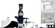
Fluorescence lifetime imaging microscope - TCS SMD FLIM
Fluorescence Lifetime Imaging Leica TCS SMD FLIM
The Leica TCS SMD FLIM system is part of the Leica TCS SMD Series. It integrates hardware and software...
The Leica TCS SMD FLIM system is part of the Leica TCS SMD Series. It integrates hardware and software...
Fluorescence lifetime imaging microscope - TCS SMD FLIM
Fluorescence Lifetime Imaging Leica TCS SMD FLIM
The Leica TCS SMD FLIM system is part of the Leica TCS SMD Series. It integrates hardware and software from PicoQuant with the high-end confocal system Leica TCS SP5 II.
It is a dedicated system for FLIM measurements. These measurements reveal information about the direct neighborhood of molecules on the nanometer scale.
FLIM is also used for binding studies (FLIM-FRET) and to identify natural metabolites under physiological conditions.
The SMD FLIM wizard optimizes FLIM measurement conditions and allows the setup of FLIM time series or FLIM stacks.
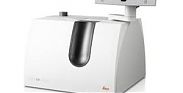
Milling system / ion beam / for sample preparation
Ion milling system Leica EM RES101
The Leica EM RES101 is a fully computer-controlled ion milling system with the...
The Leica EM RES101 is a fully computer-controlled ion milling system with the...
Milling system / ion beam / for sample preparation
Ion milling system Leica EM RES101
The Leica EM RES101 is a fully computer-controlled ion milling system with the...
The Leica EM RES101 is a fully computer-controlled ion milling system with the...