+7 (812) 645-08-06
FEM microscopes, X-ray microscopes, Electron microscopes
select brand


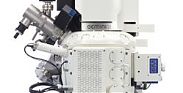
Scanning electron microscope / SEM - ZEISS EVO
The ZEISS EVO MA Series is suitable for working on a vast array of material samples. It features both beam deceleration and high definition back scattered electron imaging...
Scanning electron microscope / SEM - ZEISS EVO
The ZEISS EVO MA Series is suitable for working on a vast array of material samples. It features both beam deceleration and high definition back scattered electron imaging in order to capture topographical details at reduced voltages.
Automatic workflows will benefit from the high productivity of this series. Using specialized X-ray geometry, these EVO machines produce high resolution performance for analytical working conditions. A wide assortment of specimen sizes can be managed by the device's three different chamber sizes.
This device features a standard variable pressure operation and can be upgraded in order to observe materials in real time.
Focused ion beam system - ZEISS Crossbeam 340 & 540
The ZEISS Crossbeam 340 and Crossbeam 540 are FIB-SEMs indicated for nanotomography and nanofabrication. Using Crossbeam, imaging and analytical performance...
Focused ion beam system - ZEISS Crossbeam 340 & 540
The ZEISS Crossbeam 340 and Crossbeam 540 are FIB-SEMs indicated for nanotomography and nanofabrication. Using Crossbeam, imaging and analytical performance of the GEMINI column can be linked for sample preparation and material processing under a nanoscopic scale. Your low kV SEM performance can be combined with FIB currents up to 100 nA to speed up the nanotomography and nanofabrication. It has an easy-to-understand graphical user inerface and users can benefit from a maximum stability and a standard beam profile, making the device more reliable during complicated and long experiments.

Microscope / field emission scanning / electronic / ultra field emission scanning FE / for analysis - ZEISS MERLIN
Zeiss Merlin provides analytical capabilities for the sub-nanometer world. Merlin with the GEMINI II column is a combination of super fast analytics, high resolution imaging with excellent detection capabilities, and a future-proof flexibility of configuration in one unit.
The GEMINI II optics are prealigned. This ensures...
The GEMINI II optics are prealigned. This ensures...
Microscope / field emission scanning / electronic / ultra field emission scanning FE / for analysis - ZEISS MERLIN
Zeiss Merlin provides analytical capabilities for the sub-nanometer world. Merlin with the GEMINI II column is a combination of super fast analytics, high resolution imaging with excellent detection capabilities, and a future-proof flexibility of configuration in one unit.
The GEMINI II optics are prealigned. This ensures easy adjustment of imaging settings, like voltage or probe current, spanning several orders of magnitudes. This enables matching of application and sampling with next, without any realignment.
Excellent results in nano-analytics are provided. This is made possible with the optimization of system for high density of current, up to 300 nA probe currents, and excellent resolution at high beam currents.
Merlin provides excellent detection of parallel, on-axis and in-lens, secondary electron (SE). It also has energy selective backscattered (EsB) detection capabilities. This results in identification of the minutest differences in composition of materials, thereby generating maximum information from samples.
Merlin can be customized as per application requirements due to its modular chamber design, over 15 ports, and several other modules.
All groups of users, including novices, will find the application helpful.

VP FE-SEM microscope / SEM / electronic / ultra field emission scanning FE - ZEISS SIGMA
The SIGMA FE-SEM (Field Emission Scanning Electron Microscopes) is a series of advanced microscopes...
VP FE-SEM microscope / SEM / electronic / ultra field emission scanning FE - ZEISS SIGMA
The SIGMA FE-SEM (Field Emission Scanning Electron Microscopes) is a series of advanced microscopes used in detecting electrons.
It comes with an image navigation software which is incorporated into SmartSEM. It is designed out of the GEMINI column giving it a low voltage imaging stability. Mounting dual EDS detectors unto its chamber will increase it functionality.
It comes with an image navigation software which is incorporated into SmartSEM. It is designed out of the GEMINI column giving it a low voltage imaging stability. Mounting dual EDS detectors unto its chamber will increase it functionality.

Microscope / helium ion beam - ZEISS ORION NanoFab
The ORION NanoFab is a 3-in-1 multibeam ion microscope, designed for sub-10nm nanostructure fabrication using the NanoPatterning and Visualization Engine, and other applications....
Microscope / helium ion beam - ZEISS ORION NanoFab
The ORION NanoFab is a 3-in-1 multibeam ion microscope, designed for sub-10nm nanostructure fabrication using the NanoPatterning and Visualization Engine, and other applications. It features three beam types that users can seamlessly switch between, namely, gallium, helium and neon beams.
The gallium FIB is suitable for removing mass material in a substance sample. The helium beam, on the other hand, is ideal for fabricating sub-10 nm structures. The neon beam enables users to form nanostructures at highly efficient speeds with high throughput.
The NanoFab has a high imaging resolution of 0.5 nm, enabling high resolution images of samples using the same instrument.

TEM microscope / transmission electron - JEM-1000
Jeol's JEM 1000, the ultra high voltage transmission electron microscope that has an accelerating voltage of 1000 kV and are used in universities and research institutes across the globe. Thanks to the high accelerating voltage, the wavelength of the electrons...
TEM microscope / transmission electron - JEM-1000
Jeol's JEM 1000, the ultra high voltage transmission electron microscope that has an accelerating voltage of 1000 kV and are used in universities and research institutes across the globe. Thanks to the high accelerating voltage, the wavelength of the electrons is short which is a major parameter to consider when determining the microscope resolution with the relation d = 0.65Cs0.25?0.75, in which Cs is spherical aberration coefficient and hence high resolution is obtained regardless of the gap width of the objective lens pole piece. The high power of penetration and thick specimen observation enables to provide clear images that reveal the structures of thick specimens, which is also the biggest feature of the ultra high end microscope. Usually, the specimens for the electron microscope must be very thin and the thinned samples sometime lose the quality of the bulk materials that is conventionally used as a product. But with the advantage of an ultra high voltage, a thick specimen while having a bulk nature is observable too.
FE-SEM microscope / electronic / field emission and transmission scanning / for analysis - JEM-3200FS
The JEM-3200FS is Jeol's field emission electron microscope that features an in-column energy filter that is made within the system of imaging lens, enabling the magnification range to be almost similar to those...
TEM microscope / transmission electron - max. ø 3 mm | JEM-ARM200F
JEM-ARM200F is an Atomic Resolution Analytical Electron Microscope that includes the world's highest level STEM-HAADF resolution of 78 pm in conjunction with a STEM Cs corrector incorporated as standard. It offers the world's highest...
TEM microscope / transmission electron - max. ø 3 mm | JEM-ARM200F
JEM-ARM200F is an Atomic Resolution Analytical Electron Microscope that includes the world's highest level STEM-HAADF resolution of 78 pm in conjunction with a STEM Cs corrector incorporated as standard. It offers the world's highest level STEM-HAADF resolution of 78 pm. The JEM-ARM200F with the standard STEM Cs corrector and enhanced mechanical and electrical stability offers world's highest level STEM-HAADF resolution of 78 pm and 82 pm.
The Cs-corrected electron probe possess high current density, which is one order larger than conventional FE TEMs, which makes elemental analysis at the atomic-level with optimal enhanced throughput. With Cold FEG, with Schottky FEG direct observation of atomic column sites using TEM-ABF imaging, JEM-ARM200F provides he STEM-ABF imaging mode as standard. This technique visualizes light element column sites in crystalline samples.
The Cs-corrected electron probe possess high current density, which is one order larger than conventional FE TEMs, which makes elemental analysis at the atomic-level with optimal enhanced throughput. With Cold FEG, with Schottky FEG direct observation of atomic column sites using TEM-ABF imaging, JEM-ARM200F provides he STEM-ABF imaging mode as standard. This technique visualizes light element column sites in crystalline samples.
TEM microscope / transmission electron - JEM-2200FS
The JEM 2200FS by Jeol, which is a state of the art analytical electron microscope, comes with a 200 kV FEG or field emission gun and the omega in column energy filter that permits a zero loss image where the inelastic electrons...
TEM microscope / transmission electron - JEM-2200FS
The JEM 2200FS by Jeol, which is a state of the art analytical electron microscope, comes with a 200 kV FEG or field emission gun and the omega in column energy filter that permits a zero loss image where the inelastic electrons are eliminated, hence resulting in clearing and high contrast images while energy filtered images forming with electrons at core loss or low loss energy deliver chemical state or the elemental information of the sample. Furthermore, the spectroscopy for chemical analysis and elemental analysis is possible. The in column energy filter allows one to obtain electron energy loss spectra and energy filtered images while the optimally designed filters removes distortion in any. The JEM 2200FS which is comprised of mainly optical system, goniometer stage and evacuation system is fully PC controlled. This system produces high quality data in a stable manner.
TEM microscope / transmission electron - JEM-2100F
Jeol JEM-2100F is a multipurpose 200 kV field emission, FE, analytical electron microscope. Several versions are available to suit specific needs.
Unlike...
Unlike...
TEM microscope / transmission electron - JEM-2100F
Jeol JEM-2100F is a multipurpose 200 kV field emission, FE, analytical electron microscope. Several versions are available to suit specific needs.
Unlike conventional thermionic electron guns, a highly stable and visible electron probe is produced by the FE electron gun or FEG. This is a must for ultrahigh resolution in scanning transmission electron microscopy, or STEM, and also when analysing nano-scaled samples.
The PC system of the microscope control allows ready integration with a range of analytical devices and/or cameras. Examples include energy dispersive X-ray spectrometer, electron energy loss spectrometer or CCD cameras.

Thermal emission microscope - THEMOS
Thermal emission microscope that presents flexible system structure for micro to macro...
Thermal emission microscope - THEMOS
Thermal emission microscope that presents flexible system structure for micro to macro observation, THEMOS made an InSb camera which detects internal heat emissions from a semiconductor device, with fast and accurate solution that indicates failures in the semiconductor device. Themos mini has high cooling performance by a stirring cycle cooler.