+7 (812) 645-08-06
Scanning probe microscope / SPM / high-resolution - LEAP 4000X Si
 High Performance 3D Atom Probe for Semiconductors, Electronic Devices, and Nanomagnetics
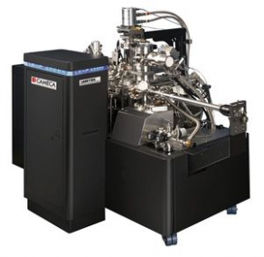
The LEAP 4000X SiTM is a high performance atom probe microscope which provides nano-scale surface, bulk and interfacial materials analysis of simple and complex structures with atom-by-atom identification and accurate spatial positioning.
The system works using the principle of field evaporation, whereby a strong electric field applied to the specimen is sufficient to cause removal of atoms by ionization. Atom removal is triggered either via a voltage or laser pulse applied to the sample.
Leap Si analysis - dopant in ultra shallow junction specimentThe LEAP Si provides the following key features:
Fastest data collection speed
Local electrode and microtip compatibility
Variable flight path
Small spot UV Laser
The system uses a UV laser with a tightly focused spot when in laser mode. The small UV laser spot enables exceptional mass resolution to be obtained. The use of UV wavelength enables a wide variety of materials, including many insulators, to be analyzed with good yield.
Local Electrode and Microtips
The name "LEAP" is derived from Local Electrode Atom Probe. The local electrode provides both ease of use and data quality as well as enabling the use of prefabricated MicrotipTM arrays. Using these enables multiple analytical specimens to be prepared, mounted and loaded into the instrument for maximum efficiency with multi-user and/or multi-experiment scenarios.